- Top
- Job Listings
- Development of single crystal growth process technology, product design, and process and equipment design for power semiconductors
JOB ID 26497
Development of single crystal growth process technology, product design, and process and equipment design for power semiconductors
- Manufacturer, Semiconductor, Electrical & Electronic, Automotive Parts
- Semiconductor, Research & Development, Production Engineer, Production Engineer
- Mie, Aichi
- ¥6,500,000~¥14,300,000
In the automotive parts industry, it is one of the largest companies in Japan in the thermal systems, mobility systems, power train systems, electrification systems, and electronic systems businesses.
We are currently focusing on four areas [electrification, connected systems, advanced safety/automated driving, and non-vehicle businesses (FA/agriculture)].
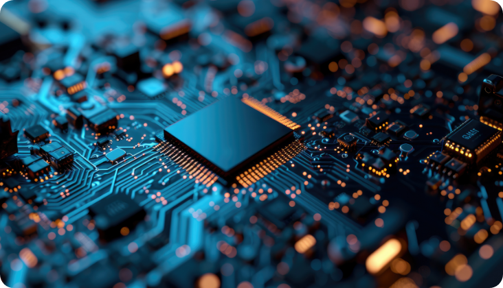
The candidate will be responsible for designing elemental and process technologies for wafer manufacturing for power semiconductors, and developing related production technologies.
Job Description
-
- Responsibilities
- Development of single crystal growth technology for power semiconductors and design of product specifications and processes
・Development of single crystal production facility control technology
・Development of production technology, facility design and process design for wafer production
・Quality assurance and control of wafer products/processes
・Negotiation with related departments, suppliers and customers inside and outside the company
・Certification of developed technologies
[Development tools]
Star-CCM (fluid analysis) ・ ANSYS (stress design)
-
- Requirements
- Semiconductor wafer product design and evaluation experience (guideline: 3 years or more)
・Inorganic material process development and process design experience (guideline: 3 years or more)
・Crystal growth technology development, production technology development and design experience (guideline: 3 years or more)
・Semiconductor wafer process design and production technology experience (guideline: 3 years or more)
・Semiconductor equipment (crystal growth, processing, epi ) development and design (Guideline: 3 years or more)
・Basic knowledge of any of inorganic materials, power electronics, or semiconductors
-
- Preferred
- Knowledge of vapor phase reaction (CVD), chemical reaction, inorganic materials and experience in development and design
- Experience and knowledge of SiC wafer manufacturing process in general
- Knowledge of power semiconductor materials and single crystal
- Experience as a promotion leader in technology development
- Experience in negotiation with overseas companies
- English proficiency (TOEIC score 610 or above as a guide, level to communicate with overseas equipment makers by e-mail and conference call) English proficiency (TOEIC score of 610 or above, level to communicate with overseas equipment manufacturers by e-mail and teleconference)
-
- Location
- Mie, Aichi
-
- Work Style
- Flex working possible
-
- Salary
- ¥6,500,000~¥14,300,000
-
- Attractive
Points - Japanese company with global opportunities, Listed company, Childcare support system, Weekends and holidays off, Major corporation
- Attractive
Consultation
Our expert team is dedicated to empowering your career change, crafting tailored career plans, and securing the best job opportunities in the automotive and mobility sectors.
Search by Industry


Search by Job Type
Search by Location
- Top
- Job Listings
- Development of single crystal growth process technology, product design, and process and equipment design for power semiconductors